 Figure 1. Visualization of a next-generation data center aisle illustrating the dense, high-performance computing environment central to modern AI infrastructure and advanced thermal management design.
Anthony Palumbo and Charles Goulding examine how 3D printed copper cold plates and in-chip microfluidic silicon are reshaping AI data center cooling, positioning copper as the rack-ready solution deployable today and in-chip microfluidics as the long-term leap, both enabled by additive manufacturing.
The Thermal Wall of AI
Every new generation of [artificial intelligence (AI)](https://www.fabbaloo.com/news/powering-the-nuclear-future-3d-printing-executive-orders-ai-infrastructure-and-the-future-of-u-s-energy…
Figure 1. Visualization of a next-generation data center aisle illustrating the dense, high-performance computing environment central to modern AI infrastructure and advanced thermal management design.
Anthony Palumbo and Charles Goulding examine how 3D printed copper cold plates and in-chip microfluidic silicon are reshaping AI data center cooling, positioning copper as the rack-ready solution deployable today and in-chip microfluidics as the long-term leap, both enabled by additive manufacturing.
The Thermal Wall of AI
Every new generation of artificial intelligence (AI) hardware pushes closer to a physical limit: heat. As trillion-parameter models and GPU-dense racks scale upward, the amount of power each data center rack consumes, and must cool, has skyrocketed. Many hyperscale deployments now exceed 100 kilowatts per rack, a figure that air-cooling systems can no longer handle.
Conventional heat exchangers, known as cold plates, circulate coolant through metal channels mounted to processors. They have served reliably for decades, but at these power densities, even the best machined or brazed designs are reaching their thermal ceiling. Uniform flow becomes difficult to maintain, seams introduce leak risks, and pumping power rises steeply as engineers push more fluid through narrower channels.
As a result, data center cooling has transformed from a background utility into a core design constraint. The Open Compute Project (OCP), a consortium that defines hardware and cooling standards for hyperscale operators, now targets liquid-cooling readiness as a baseline requirement for new racks. Yet, even with liquid cooling, today’s systems are nearing their upper threshold. The next leap demands a fundamental redesign of how heat moves, from transistor to coolant loop.
How Data Centers Move Heat
To understand why this challenge is so significant, it helps to follow the path that heat takes through a system. It begins deep inside the silicon die, where billions of transistors switch on and off trillions of times per second. Each switching event releases a trace of heat, and collectively, they produce power densities that can exceed 1,000 watts per square centimeter (W/cm2) during AI workloads.
That heat travels outward through a layered thermal stack: from the silicon die into a thermal interface material (TIM), across a metallic lid or heat spreader, and finally into a cold plate, where a circulating liquid coolant carries it away. Each of these layers introduces thermal resistance (°C/W), representing how much temperature rises as power flows through. A small inefficiency in any layer can raise chip temperatures dramatically.
Once inside the cold plate, the coolant (often a water–glycol mixture) absorbs the heat through convection. The system’s performance depends on two opposing factors: heat flux (how much heat can be transferred through a given area) and pressure drop (how much energy it takes to push coolant through narrow channels). Narrower microchannels restrict surface contact and heat transfer but also restrict flow, demanding more pump power. Achieving balance between these parameters defines the efficiency of the entire system, a trade-off detailed in an IBM/ITherm study on embedded liquid cooling with microstructures.
Traditionally, engineers have been limited by manufacturing. Milling and brazing can only produce straight or planar channels, which lead to uneven flow and thermal “hot spots.” Additive manufacturing changes this equation by allowing non-planar, lattice-like geometries that match coolant flow to the heat distribution of each processor. Using computational fluid dynamics (CFD) simulations, engineers can model pressure, velocity, and turbulence before printing a single prototype.
Beyond the chip, the same principles apply at scale. Coolant circulates through manifold loops that distribute fluid through multiple racks, returning it to facility-level heat exchangers. Industry standards like the OCP ensure compatibility between systems by defining connector sizes, flow rates, and coolant types. This standardization is essential, as any new technology must integrate seamlessly into existing liquid loops.
Two Paths to the Same Goal
The challenge of heat management has produced two radically different engineering paths that share the same destination: efficient, scalable thermal transfer. The first relies on 3D printed copper cold plates, where additive manufacturing transforms the geometry of heat exchange. The second embeds microfluidic channels directly into silicon chips, bringing coolant within microns of the transistors themselves
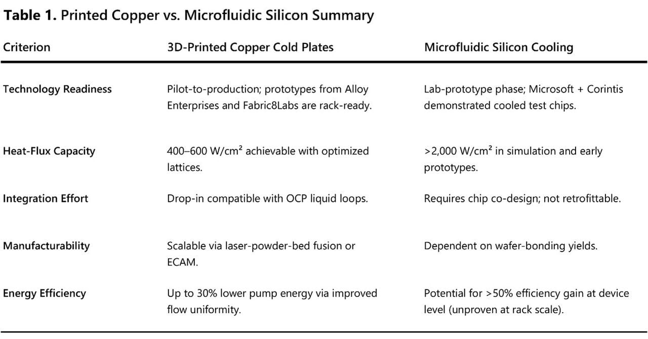
Printed Copper: The Deployable Frontier
For today’s data centers, 3D printed copper is the most practical and scalable option. Additive manufacturing enables engineers to merge thermal physics with geometric freedom, printing intricate flow networks, variable fin densities, and conformal lattices that distribute coolant precisely where heat concentrates.
Alloy Enterprises has demonstrated a cold plate dissipating 4 kilowatts (kW) at 4 liters per minute (L/min) of PG25 coolant (a 25% propylene-glycol blend) at a 44 °C inlet temperature, achieving equivalent cooling at roughly one-third less flow than the OCP baseline. Using C110 copper, known for its 99.9% conductivity, improved performance by about 30% over aluminum designs while maintaining corrosion compatibility.
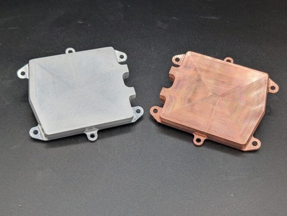 Figure 2. Alloy Enterprises’ single-piece, leak-tight aluminum (left) and copper (right) cold plate components demonstrated ~4.35 kW dissipation at 4 L/min PG25; ~33% lower flow than OCP’s baseline for equivalent cooling. (Source: Alloy Enterprises)
A parallel advance comes from Fabric8Labs, whose Electrochemical Additive Manufacturing (ECAM) process builds dense copper parts via room-temperature electroplating, without powders or lasers. The method produces sealed internal manifolds suitable for data center-grade cold plates and can scale to high volumes. Demonstrated publicly at Computex and OCP 2025, ECAM represents AM’s shift from prototyping to production-scale thermal hardware. Recent funding underscores how quickly this platform is scaling. In November 2025, Fabric8Labs raised a new US$50 million funding round to expand its U.S.-based ECAM manufacturing capacity. This is ramping from about 5 million to 22 million components per year across thermal management, RF, and power electronics programs.
Real-world demonstrations are already appearing. Wiwynn and Meta have tested OCP-compatible printed plates that integrate directly into existing coolant loops, showing measurable reductions in pump energy and more uniform temperature distribution. The combination of manufacturability, compatibility, and immediate efficiency gains make additive copper the deployable frontier of data center cooling, representing a bridge between current infrastructure and future architectures.
Microfluidic Silicon: Cooling Inside the Chip
If printed copper reimagines the cold plate, microfluidic silicon redefines the chip itself. Instead of pulling heat away from the die, this approach routes coolant through channels etched directly beneath the transistor layer, eliminating traditional barriers like lids and interface materials. The coolant flows within hair-width passages, absorbing heat almost at the moment it’s generated.
In September 2025, Microsoft and Corintis unveiled prototypes showing up to 3× greater heat removal and ~65% lower GPU peak temperatures in simulation compared to conventional packaging. These designs target heat flux densities beyond 2,000 W/cm², far exceeding the limits of external cold plates.
The engineering challenges are formidable. Embedding coolant requires wafer bonding, where two silicon layers are fused to seal microchannels with micron precision. Any contamination, void, or misalignment can destroy an entire wafer. Coolant chemistry and filtration become critical when microscopic debris could clog a channel, and any leak would instantly short the die. Still, the progress is accelerating: Corintis’s US$24 million Series A is funding pilot production of one million cooled chips per year by 2026, supported by new foundry partnerships.
Research institutes such as IBM Zurich, CEA-Leti, and Empa are already demonstrating test wafers handling sustained ultra-high heat flux near 1,800 W/cm². Though commercial deployment remains years away, the concept has proven its physics, with its potential to make cooling a built-in semiconductor function rather than an external system.
Where the Two Worlds Meet
The line between printed copper and microfluidic silicon is beginning to blur. Engineers are developing hybrid architectures that use additively manufactured copper manifolds to feed coolant directly into stacked silicon dies. These manifolds act as pressure-equalizing bridges, ensuring consistent flow across hundreds of microscopic channels without leakage or material mismatch.
New additive interposers, such as thin copper transition layers, connect wafer-level microchannels to rack-scale plumbing while helping manage thermal-expansion mismatches between metal and silicon. Early research studies report large reductions in overall thermal resistance compared to conventional plate systems, exceeding 50% in optimized manifold microchannel designs. The OCP is already discussing standards to certify these geometries, a step that could make hybrid cooling modules commercially interchangeable across vendors.
In this hybrid model, additive manufacturing becomes not just a product technology but an enabling infrastructure, forming the precision plumbing through which silicon-scale cooling becomes practical at data center scale. Recent hybrid prototypes that combine copper structures with silicon 3D manifolds illustrate the direction of travel from lab to pilot production.
The New Language of Thermal Design
What makes these advances remarkable isn’t only their performance, it’s how they blend once-separate engineering disciplines into a single design ecosystem. Thermal management now draws simultaneously from materials science, fluid mechanics, and semiconductor packaging, united by the same digital design pipeline.
Additive manufacturing sits at the center of this convergence. It allows engineers to translate CFD simulations directly into hardware, revise designs through software rather than tooling, and validate performance with rapid iteration cycles. Each printed iteration informs the next, shortening development timelines while reducing material waste. This digital-to-physical loop aligns with data center sustainability goals, where efficiency gains in cooling translate directly into reduced energy use and lower carbon intensity.
Cooling has thus evolved from a static component into a design discipline, a language of lattices, flow fields, and material interfaces that defines the limits of computation itself.
The Research & Development Tax Credit
The now permanent Research and Development (R&D) Tax Credit is available for companies developing new or improved products, processes, and/or software. 3D printing can help boost a company’s R&D Tax Credits. Wages for technical employees creating, evaluating, and revising 3D printed prototypes are typically eligible expenses toward the R&D Tax Credit. Similarly, when used as a method of improving a process, time spent integrating 3D printing hardware and software can also be an eligible R&D expense. Lastly, when used for modeling and preproduction, the costs of filaments consumed during the development process may also be recovered.
Whether it is used for creating and testing prototypes or for final production, 3D printing is a great indicator that R&D Credit-eligible activities are taking place. Companies implementing this technology at any point should consider taking advantage of R&D Tax Credits.
Conclusion: Cooling as the Bottleneck and the Breakthrough
Data centers are entering a new thermal reality. 3D-printed copper provides the bridge from today’s systems to the next generation, offering immediate, manufacturable gains. Microfluidic silicon points toward the long-term horizon, where heat removal becomes intrinsic to the processor.
Between them lies a shared foundation: additive manufacturing. The technology capable of shaping coolant paths, bonding interfaces, and design iteration cycles at every scale.
In the race to sustain AI’s exponential growth, heat has become both the bottleneck and the opportunity. The future of computing won’t just be powered by silicon; it will be cooled, connected, and ultimately manufactured additively.