 Electrophotographic powder printing process [Source: PatentScope]
A new patent outlines an electrophotographic powder process that flips powder polarity between layers to curb charge build-up and enable cleaner, denser prints.
Electrophotographic deposition borrows from laser printing to handle powders with a charged photoconductor, then transfers material to the part. It should allow for precise placement and low waste, but persistent electrical charge in the growing stack can repel incoming powder, limit layer count, and erode reliability. This application proposes a simple remedy: alternate the charge polarity of successive powder fractions so each new layer attracts rather than repels …
Electrophotographic powder printing process [Source: PatentScope]
A new patent outlines an electrophotographic powder process that flips powder polarity between layers to curb charge build-up and enable cleaner, denser prints.
Electrophotographic deposition borrows from laser printing to handle powders with a charged photoconductor, then transfers material to the part. It should allow for precise placement and low waste, but persistent electrical charge in the growing stack can repel incoming powder, limit layer count, and erode reliability. This application proposes a simple remedy: alternate the charge polarity of successive powder fractions so each new layer attracts rather than repels the previous one.
The patent covers polymers, ceramics and even metals with dielectric coatings, and permits several powders to be combined in a single build. It sets up the work as an alternative to powder bed systems like Selective Laser Sintering (SLS) and HP’s Multi Jet Fusion (MJF), and adjacent to commercial electrophotographic approaches in thermoplastics.
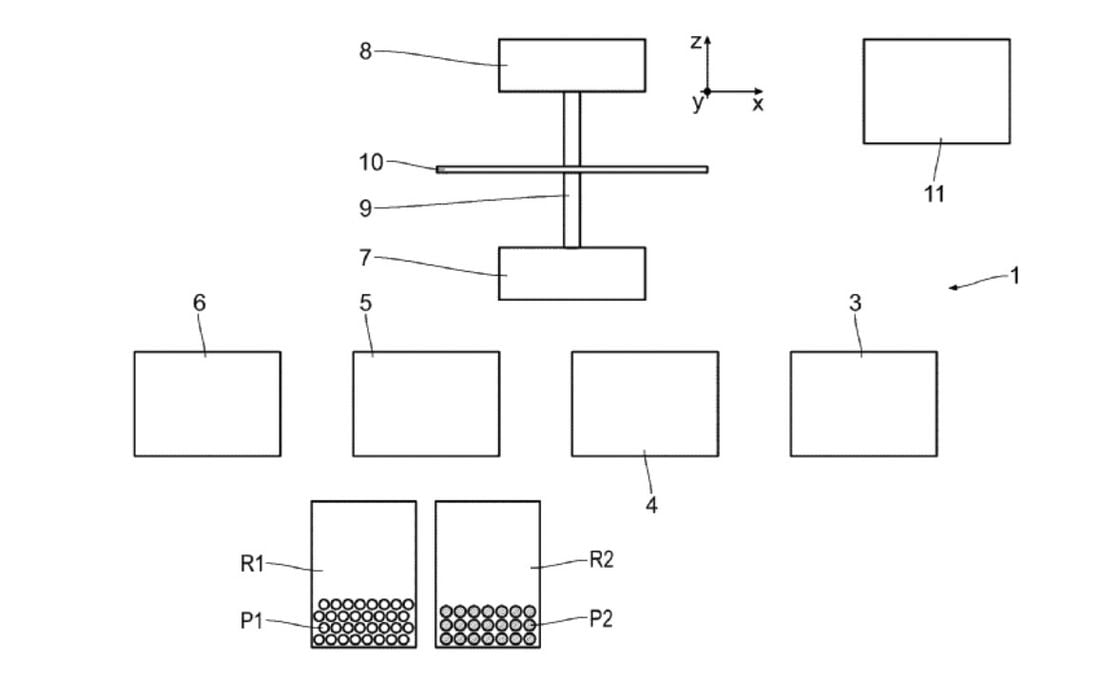
The apparatus cycles a deposition unit through charging, exposure, developing and printing stations. A photoconductive layer is charged, then selectively discharged by LED exposure to define where powder should adhere. Powder is charged by corona or a triboelectric magnetic brush and is picked up without contact by the deposition unit before being transferred to the build.
Alternating Polarity Tackles Charge Build-Up
The core mechanism is very straightforward. Successive powder fractions are charged with opposite polarity. That neutralizes surface potential growth in the stack and turns repulsion into attraction at the layer interface. The patent also suggests measuring the surface potential and flipping polarity when a limit is reached, around one thousand volts, to keep transfer stable.
Pickup, holding and deposition are driven by a reversible high-voltage supply on a conductive base plate behind the photoconductor. A grounded transfer structure — essentially a copper frame surrounding the deposition unit — shapes the electric transfer field so powder jumps across a set gap to the deposition surface. The process supports white writing or black writing modes depending on whether powder adheres to exposed or unexposed regions.
To further boost reliability, the deposition unit can be vibrated by a piezo actuator at frequencies between one hundred hertz and twenty kilohertz. The patent recommends triggering vibration only after the transfer field is fully established, which reduces false prints and improves coverage.
Thicker Layers And Multi-Material Potential
A notable claim in the patent is throughput. Triboelectric charging is said to charge thicker powder layers uniformly, letting the system pick up layers roughly two to five particle diameters thick — for example about sixty to three hundred microns — compared to gas discharge that is often limited to about sixty to one hundred twenty microns. If realized, that could raise part throughput while preserving fine features where needed by dialing down local layer thickness.
The deposition unit includes fluid channels for heat transfer oil to preheat powder close to, but below, its melting temperature and within a quasi-isothermal window between recrystallization and melting. The build chamber can be held in the same window — for PA12 the patent cites roughly 158C to 181C, for PA11 roughly 164C to 199C — which helps avoid curling and lets users tune crystallinity for mechanical properties.
The method is clearly aimed at multi-material AM. It allows different powders to be deposited within a single layer (same polarity within the layer) or across layers (alternating polarity between layers). The patent suggests combinations like PA12 with TPU to localize stiffness and elasticity in one print without adhesive joints. Metal and ceramic use would rely on selective energy input or binder jet style green parts with debinding and sintering.
There are some unknowns, including the photoconductor material cited, arsenic selenide, raises durability and EHS questions in a hot chamber. Corona systems can generate ozone; filtration and maintenance will matter. Build volume, cycle time per layer, material property data, and end-to-end automation metrics are not stated. Metal powders require dielectric coatings, and software for voxel-level toolpaths across materials will determine practical adoption.
Real proof will come from repeatability data, coverage uniformity at different gap distances, and long-run operation without photoconductor damage. If the polarity alternation truly eliminates charge-driven failure modes while enabling thicker layers, service bureaus chasing polymer blends — footwear, orthotics, consumer goods — could be early beneficiaries. Competition with existing electrophotographic offerings will hinge on material breadth and uptime rather than pure physics.
If electrophotography can finally tame static, powder-bed AM gains a surprising new knob: polarity.
Via Google Patents

By Kerry Stevenson
Kerry Stevenson, aka "General Fabb" has written over 8,000 stories on 3D printing at Fabbaloo since he launched the venture in 2007, with an intention to promote and grow the incredible technology of 3D printing across the world. So far, it seems to be working!
View all of Kerry Stevenson’s posts.