Hyperscalers prioritize inference efficiency and cost (40-50% reductions). By 2028, custom ASICs could capture 20-30% market from Nvidia’s ~90%, with total AI chip sales ~$975B in 2026.
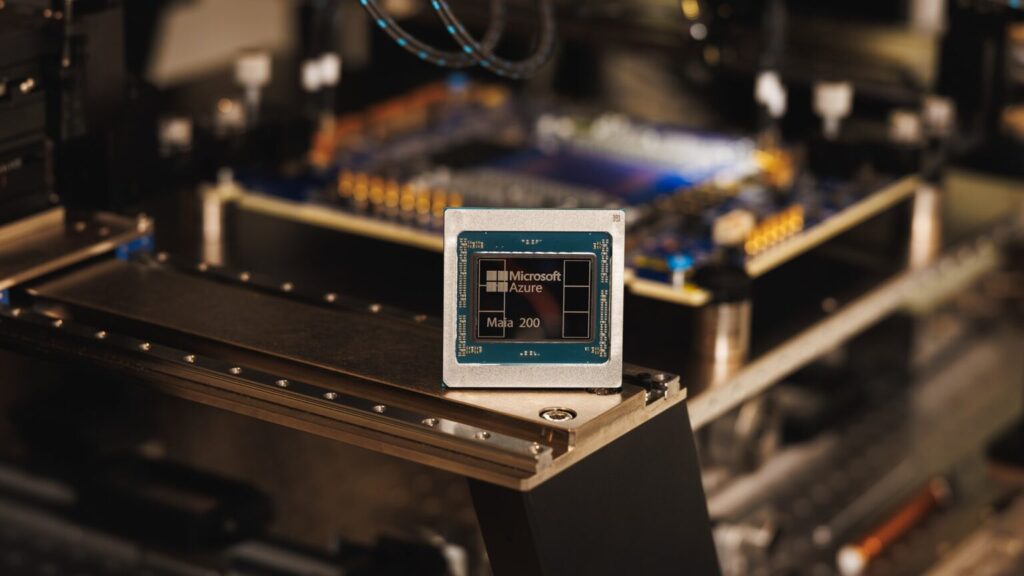
It has native FP8/FP4 tensor cores, a redesigned memory system with 216GB HBM3e at 7 TB/s and 272MB of on-chip SRAM, plus data movement engines that keep massive models fed, fast and highly utilized. This makes Maia 200 the most performant, first-party silicon from any hyperscaler, with three times the FP4 performance of the third generation Amazon Trainium, and FP8 performance above Google’s seventh generation TPU. Maia 200 is also the most efficient inference system Microsoft has ever deployed, with 30% better performance per dollar than the latest generation hardware in our fleet today.
Maia 200…
Hyperscalers prioritize inference efficiency and cost (40-50% reductions). By 2028, custom ASICs could capture 20-30% market from Nvidia’s ~90%, with total AI chip sales ~$975B in 2026.
It has native FP8/FP4 tensor cores, a redesigned memory system with 216GB HBM3e at 7 TB/s and 272MB of on-chip SRAM, plus data movement engines that keep massive models fed, fast and highly utilized. This makes Maia 200 the most performant, first-party silicon from any hyperscaler, with three times the FP4 performance of the third generation Amazon Trainium, and FP8 performance above Google’s seventh generation TPU. Maia 200 is also the most efficient inference system Microsoft has ever deployed, with 30% better performance per dollar than the latest generation hardware in our fleet today.
Maia 200 is part of Microsofts heterogenous AI infrastructure and will serve multiple models, including the latest GPT-5.2 models from OpenAI, bringing performance per dollar advantage to Microsoft Foundry and Microsoft 365 Copilot. The Microsoft Superintelligence team will use Maia 200 for synthetic data generation and reinforcement learning to improve next-generation in-house models. For synthetic data pipeline use cases, Maia 200’s unique design helps accelerate the rate at which high-quality, domain-specific data can be generated and filtered, feeding downstream training with fresher, more targeted signals.
Maia 200 chip contains over 140 billion transistors and is tailored for large-scale AI workloads while also delivering efficient performance per dollar. It is designed for the latest models using low-precision compute, with each Maia 200 chip delivering over 10 petaFLOPS in 4-bit precision (FP4) and over 5 petaFLOPS of 8-bit (FP8) performance, all within a 750W SoC TDP envelope. In practical terms, Maia 200 can effortlessly run today’s largest models, with plenty of headroom for even bigger models in the future.
 Screenshot
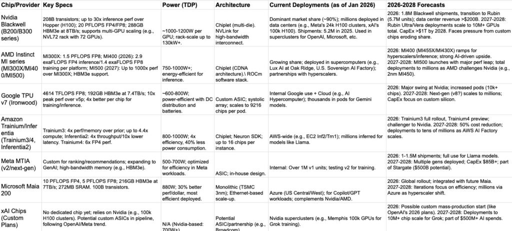
The AI boom is dominated by Nvidia’s Blackwell GPUs, which attract significant investor interest. AMD’s MI series is gaining market share as a competitor. Google’s TPU (now on v7 Ironwood) is deployed internally; more details available in a related AI hardware show on the channel.
Hyperscalers are developing custom chips.
Meta’s MTIA (training and inference accelerator) has produced over a million units successfully, with a next-gen version planned. Amazon’s Trainium (chiplet design with HBM) and Inferentia chips gained traction in late 2025. Building chips is complex (design, physical implementation, supply chain), so hyperscalers often partner with firms like Broadcom, MediaTek, or Marvell for faster time-to-market. XAI if working on AI5/ AI6 /AI7 and AI8.
Microsoft
A couple of years ago, Microsoft launched the Maia AI chip and Cobalt CPU. Maia (contains “AI” in the name) is for AI acceleration; Cobalt is an ARM-based CPU host. Competitors: Google’s Axion and Amazon’s Graviton CPUs.
Cobalt 200
Announced in November 2025. Features two chiplets with 66 Arm Neoverse V3 cores each (or tweaked versions), totaling up to 132 cores. Potential for binning (variations in core count based on manufacturing yields).
Maia 200 Successor to Maia 100, positioned against Nvidia. Focused on inference for data centers. Built on TSMC’s 3nm process with native FP8 and FP4 tensor cores. Specs are 216 GB HBM3 at 7 TB/s bandwidth, 272 MB on-chip SRAM. Monolithic die with six HBM3E stacks (likely SK Hynix 12-high 64 GB dies at 9200 MT/s).
Performance
Claims 3x FP4 performance vs. Amazon’s third-gen Trainium; most efficient inference system Microsoft has deployed, with 30% better performance per dollar over existing systems (including Nvidia and AMD). Deployment starting in US Central, then US West 3 (Phoenix, Arizona), and other regions. Die details: 100 billion transistors, ~727 mm² area on TSMC N3E; SRAM occupies 10-12% of the chip (6-transistor cells, above average density). Peak performance: 10 PFLOPS FP4, ~5 PFLOPS FP8; 880W TDP (20W more than Maia 100). System: Four chips per blade server; redesigned memory subsystem for narrow precision, specialized DMA engine, SRAM, and NoC for high-bandwidth data. Comparisons: 4x peak FP4 TOPS vs. Trainium 3; more FP8 TOPS than Google’s TPU v7; more memory than both, but slightly lower bandwidth than TPU v7; better scale-up bandwidth with two-tier design.
Networking and Scale-Up Design
28 x 400 GB Ethernet ports per chip (four-chip blade); likely 7 links per chip within blade and 7 out. Uses standard Ethernet with a custom Azure protocol optimized for low-bit precision data types and reduced power. Much of the chip’s shoreline dedicated to these links.
Rack-Scale Architecture
Microsoft Rack design resembles Nvidia’s NVL72. 18 blades with 4 chips each = 72 compute chips per rack. Switches in the middle and it was co-developed with Marvell. It maybe using Teralynx 10 for switch blades. Includes Cobalt 200 blades for CPU and management. Total power is ~65 kW per rack. Liquid-cooled (880W chips). Instances offered via cloud, not full racks.
SDK with Triton compiler, PyTorch support, low-level NPL programming, simulator, and cost calculator; architecture details sparse (likely systolic array evolution of Maia 100).
Monolithic vs. Chiplet Design
Monolithic design (vs. chiplet approaches like Amazon’s latest training platform). Relies on TSMC N3P for large silicon, with binning for frequency, TOPS, and ALUs.