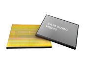
This afternoon, a ZDNet South Korea news article has disclosed early details of another intriguing 2 nm project reportedly underway at Samsung Semiconductor. Specific customers are not mentioned by industry insiders, but the South Korean megacorporation’s HBM (High Bandwidth Memory) development team could be tailoring custom logic dies for individual product requirements. There are rumors circulating about the computer memory R&D department selecting "foundry process nodes as advanced as 2 nm" for next-wave HBM designs. The ZDNet piece does not define whether engineers have opted into using the in-house foundry’s SF2 or SF2P nodes.
Samsung’s sixth-gen HBM product line (aka HBM4) is said to be based on a 4 nm process node, likely picked out from the SF4 family. Ac…
This afternoon, a ZDNet South Korea news article has disclosed early details of another intriguing 2 nm project reportedly underway at Samsung Semiconductor. Specific customers are not mentioned by industry insiders, but the South Korean megacorporation’s HBM (High Bandwidth Memory) development team could be tailoring custom logic dies for individual product requirements. There are rumors circulating about the computer memory R&D department selecting "foundry process nodes as advanced as 2 nm" for next-wave HBM designs. The ZDNet piece does not define whether engineers have opted into using the in-house foundry’s SF2 or SF2P nodes.
Samsung’s sixth-gen HBM product line (aka HBM4) is said to be based on a 4 nm process node, likely picked out from the SF4 family. According to an anonymous company insider: "Samsung Electronics is designing a custom logic die for HBM under the leadership of the custom SoC (system-on-chip) team newly established within the System LSI Business Division last year…We are building a portfolio ranging from 4 nm to 2 nm to respond to the needs of various customers." ZDNet adds that next-gen ultra-high-performance AI accelerators are expected to rely on the very best futuristic HBM modules. "Strong" AI enterprise industry demand is anticipated once 2 nm logic dies come into fruition, possibly post-2027, after the arrival of HBM4E (seventh gen).


