Neuromorphic computing represents a rapidly advancing computational paradigm inspired by the structural and functional mechanisms of the human brain [1]. This approach has garnered significant attention for its promising applications in artificial intelligence (AI) due to its potential to surpass conventional deep learning frameworks in terms of energy efficiency and computational speed. By mimicking the parallel and event-driven nature of human neural systems, neuromorphic computing offers an alternative approach to address the growing demands for efficient AI processing. However, despite its immense potential, several significant challenges remain in realizing practical, large-scale neuromorphic system.
Neuromorphic system achieves high-speed and low-power arti…
Neuromorphic computing represents a rapidly advancing computational paradigm inspired by the structural and functional mechanisms of the human brain [1]. This approach has garnered significant attention for its promising applications in artificial intelligence (AI) due to its potential to surpass conventional deep learning frameworks in terms of energy efficiency and computational speed. By mimicking the parallel and event-driven nature of human neural systems, neuromorphic computing offers an alternative approach to address the growing demands for efficient AI processing. However, despite its immense potential, several significant challenges remain in realizing practical, large-scale neuromorphic system.
Neuromorphic system achieves high-speed and low-power artificial neural networks using dedicated hardware. This approach requires the neuronal circuit elements that exhibit nonlinear input–output characteristics emulating the behavior of biological neurons’ activation functions. Furthermore, the construction of large-scale networks equipped with adjustable synaptic weights is essential to realize practical ANNs. Such networks must be capable of dynamic reconfiguration and fine-grained modulation of synaptic strengths to effectively support complex learning tasks. The combined advancement of neuronal and synaptic device technologies will be crucial for the widespread deployment of neuromorphic computing in next-generation AI applications.
Research has been carried out on circuit implementation of ANNs using various devices. For instance, CMOS-based neuromorphic chips benefit from mature fabrication processes, enabling high-density integration. However, they often suffer from relatively high-power consumption and limited capacity to emulate complex biological neuronal dynamics [2–5]. Moreover, realizing nonlinear neuronal properties using only CMOS circuits poses a significant challenge. Memristor-based approaches offer promise due to their low power operation and non-volatility, enabling dense and energy-efficient synaptic implementations, although they are hindered by challenges related to linearity, endurance, and device variability [6–8]. Neural networks built upon spintronic devices, which harness electron spin for information processing, offer promising avenues for achieving high-speed and low-energy computation [9–12]. Nevertheless, the exclusive construction of an entire neural network solely from spin devices remains a significant challenge. When these spintronic components are hybridized with conventional semiconductor integrated circuits, the overall system’s performance can be constrained by the interface circuits bridging the two technologies. Optical neuromorphic systems, capitalizing on the inherent parallelism and speed of light, demonstrate remarkable potential for high bandwidth and low latency, though they encounter difficulties concerning scalability and integration with conventional electronic components [13, 14].
Among various device technologies, superconductive circuits, which offer ultra-fast operational speeds and extremely low power dissipation, are thought to be suitable for implementing ANN hardware. In single flux quantum (SFQ) logic [15, 16], binary information is represented by quantized magnetic flux propagating as voltage pulses—termed SFQ pulses—at the speed of light, facilitating operation frequencies approaching the terahertz regime [17, 18]. Furthermore, the pulse-based transmission mechanism in SFQ circuits bears resemblance to action potentials in biological neurons, suggesting their strong suitability for neuromorphic applications [19]. The availability of low-cost, fast random number generation is another advantage of ANNs with SFQ circuits [20, 21]. While SFQ-based neuromorphic circuits offer significant advantages in terms of speed and power, existing designs have faced specific limitations.
We proposed an SFQ-based neuron circuit with sigmoid activation functions in 2013 [22]. This circuit utilizes the sigmoidal output characteristic of Josephson current comparators [23, 24] and can operate at speeds above 10 GHz. However, its large circuit area, resulting from the use of a low-pass filter to convert high-frequency SFQ pulses into DC current, poses a significant limitation. Specifically, the footprint of the SFQ sigmoid neuron is 0.9 mm × 1.4 mm [22], which makes integrating a large number of neurons unfeasible. Other studies on sigmoidal neuron elements based on superconducting circuits [25–29] share this disadvantage of requiring a substantial circuit area.
Furthermore, the sigmoid activation presents substantial challenges in the context of training deep neural networks, particularly when using backpropagation algorithms [30]. A principal difficulty lies in the vanishing gradient problem: as the activation function’s gradient diminishes, weight updates become correspondingly small, thereby impeding effective training, especially in deeper networks. The maximum gradient of the sigmoid function, approximately 0.25, exacerbates this phenomenon. The rectified linear unit (ReLU) activation function, with its constant gradient for positive inputs, offers a promising solution to mitigate this vanishing gradient issue, enabling more effective training of deep networks.
Another significant challenge in the realization of ANN hardware is device parameter variation. When a large number of neuron elements are integrated, variations in their properties arising during fabrication can degrade the performance of the entire ANN system. This issue is particularly pronounced in neuronal elements based on the analog components discussed above. Although the impact of device parameter variation on ANN performance based on various circuit devices has been quantitively investigated [31, 32], no fundamental solution has yet been achieved. Furthermore, in ANNs with superconducting circuits, which are ultra-sensitive to current and magnetic flux, the device parameter variation can have a significant impact on performance.
In this work, we propose a novel compact superconductive neuron device that implements the ReLU activation function, which can solve the problems caused by the vanishing gradient problem. The proposed circuit realizes the ReLU input–output characteristic through frequency conversion between input and output signals, based on digital information processing by an SFQ logic circuit. A key advantage of our design, directly addressing the limitations of previous analog-based approaches, is its remarkable robustness against device variability due to the inherent digital nature of SFQ logic. Even with approximately up to 20% variation among individual circuit parameters, the circuit achieves the ideal ReLU input–output characteristic. This robustness sharply contrasts with conventional analog-based neuron devices, whose performance is highly sensitive to device nonuniformity, and represents a major step toward the scalable integration of superconducting neural networks.
We report on the implementation of the proposed neuron circuit using the 10 kA cm2 Nb four-layer process and present experimental demonstrations of its high-speed operation, achieving an input frequency of 40 GHz. This work demonstrates a significant advancement towards realizing highly scalable and robust superconducting neuromorphic systems for next-generation AI applications.
We introduce the operating principle and features of the SFQ circuit briefly. Figure 1(a) shows an equivalent circuit diagram of an SFQ delay flip-flop (DFF) with escape function (DFFE) and its input/output characteristics. The SFQ DFFE has two states, ‘0’and ‘1’ corresponding to the state where no magnetic flux quantum ( , where h is the Planck constant and e is the electron charge) is stored in the circuit, and the state where a flux quantum is stored, respectively. A Josephson junction is a circuit element that switches and propagates a magnetic flux quantum when the current flowing through it exceeds the critical current. An SFQ input from the ‘din’ port in figure 1(a) induces the switching of Josephson junction J1, and the input magnetic flux quantum is stored in the superconducting loop composed of J1, Ls, and J2. This corresponds to a transition from the ‘0’ state to the ‘1’ state. The stored magnetic flux quantum induces a circulating current, which causes a current to flow in J2, making J2 easier to switch. When a ‘clock’ signal is input in ‘1’ state, J2 switches and the stored magnetic flux quantum is output to the ‘dout’ port. At this time, the DFF is initialized to the ‘0’ state. When the DFFE is in the ‘0’ state, the input ‘clock’ signal is canceled by the switching of J3. The input din signal is canceled by the switching of Je when the DFFE is in the ‘1’ sate. By adjusting the circuit structure and device parameters in this way, various SFQ logic gates can be realized [16].
Figure 1. (a) Equivalent circuit and timing diagram of the SFQ delay flip-flop with escape junction (DFFE) J1, J2, J3, and Je represent Josephson junctions. In the SFQ circuit, ‘1’ and ‘0’ are expressed by the presence and absence of voltage pulse, which corresponds to a voltage generated according to Faraday’s law of electromagnetic induction when a magnetic flux quantum crosses the junction. Circuit symbols and state transition diagrams of (b) DFFE and (c) resettable delay flip-flop (RDFF).
Download figure:
Standard image High-resolution image 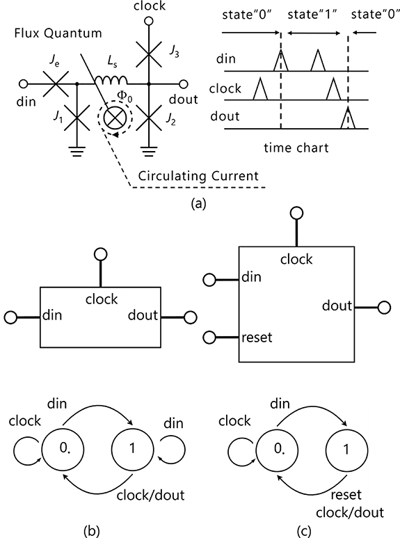
In biological neural systems, higher input signal frequencies are generally interpreted as stronger or more salient stimuli. Motivated by this principle, neuromorphic circuits based on SFQ technology can encode signal magnitude using the frequency of SFQ pulses. This frequency-domain representation allows the circuit behavior to more closely emulate biological information processing [1].
Figures 1(b) and (c) illustrates the symbols and state transition diagrams of the DFFE and resettable DFF (RDFF) used in the proposed neuron circuit. The RDFF plays a central role in the proposed circuit in this study. When an SFQ signal is applied to the ‘reset’ port of the RDFF while it is in its ‘1’ state, the stored flux is released, and the state switches to the ‘0’ state without outputting an SFQ signal. This operation can be considered as the ‘reset’ input canceling the ‘din’ input. We implement a neuron circuit with ReLU activation using this resetting function on the RDFF.
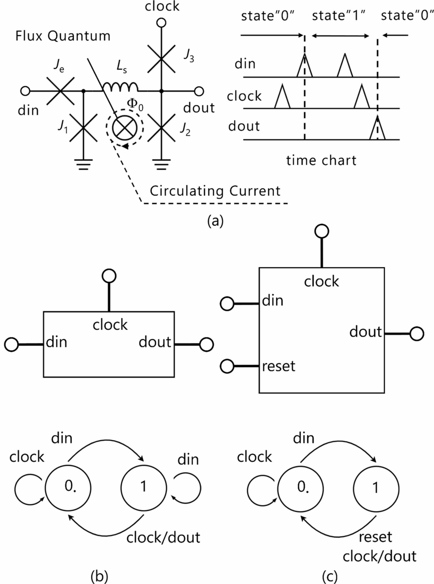
Figure 2(a) shows a block diagram of the superconductive neuron with ReLU activation function. In this circuit, periodic SFQ signals are input from the ‘input’ and ‘cancel’ ports at frequencies of fin and fcan, respectively. The ‘input’ SFQ signal is split and input to ‘din’ and ‘clock’ ports of the RDFF and ‘clock’ port of DFFE. The ‘clock’ input for the RDFF is delayed by Josephson transmission line [16], which has the propagation delay of 20.8 ps in our design, and always input to the RDFF after ‘din’ input. The DFFE is inserted before ‘din’ input of RDFF for adjusting the timing of ‘reset’ input to the RDFF. Figure 2(b) shows the RDFF’s timing diagram with output. When an SFQ signal is input to the ‘input’ port, the RDFF’s internal state transitions to ‘1’ by the ‘din’ input. A subsequent, delayed clock signal then causes an SFQ signal to be output from the ‘output’ port. Figure 2(c) shows the RDFF’s timing diagram without output. If an SFQ signal is applied to the ‘input’ port after the DFFE has transitioned to the ‘1’ state due to a ‘cancel’ input, an SFQ signal is fed to ‘reset’ port of the RDFF following the ‘din’ input. This action immediately resets the RDFF to the ‘0’ state after a momentary ‘1’ state. Consequently, no output is generated even when an SFQ signal is subsequently applied to ‘clock’ port of the RDFF.
Figure 2. (a) Block diagram of the proposed neuron circuit, and RDFF’s timing diagram (b) without cancel input and (c) with cancel input.
Download figure:
Standard image High-resolution image 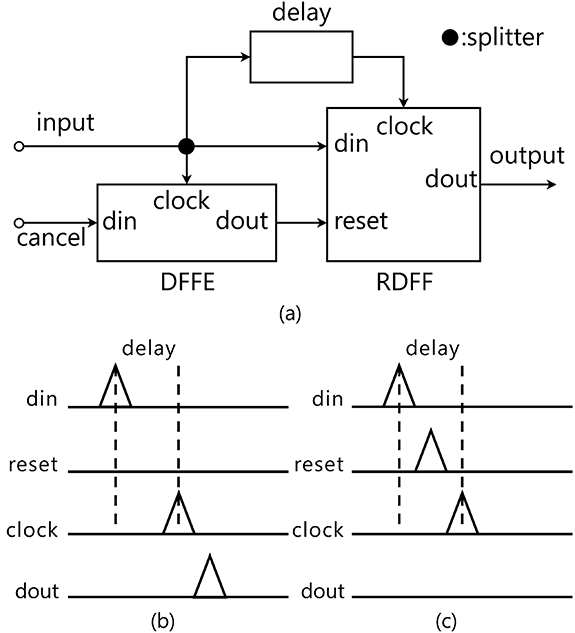
Based on this operation, in the case of  , the SFQ signal is output to the ‘output’ port at the frequency of the difference between fin and fcan (
 ), because the ‘input’ is cancelled by the ‘cancel’ inputs with the probability of
  . When
  , no output is obtained since the RDFF always receives a ‘reset’ input before the ‘clock’ input after the ‘din’ input. This functionality corresponds to a biased ReLU function, defined as:

where fout is the average SFQ signal frequency obtained from ‘output’ port.
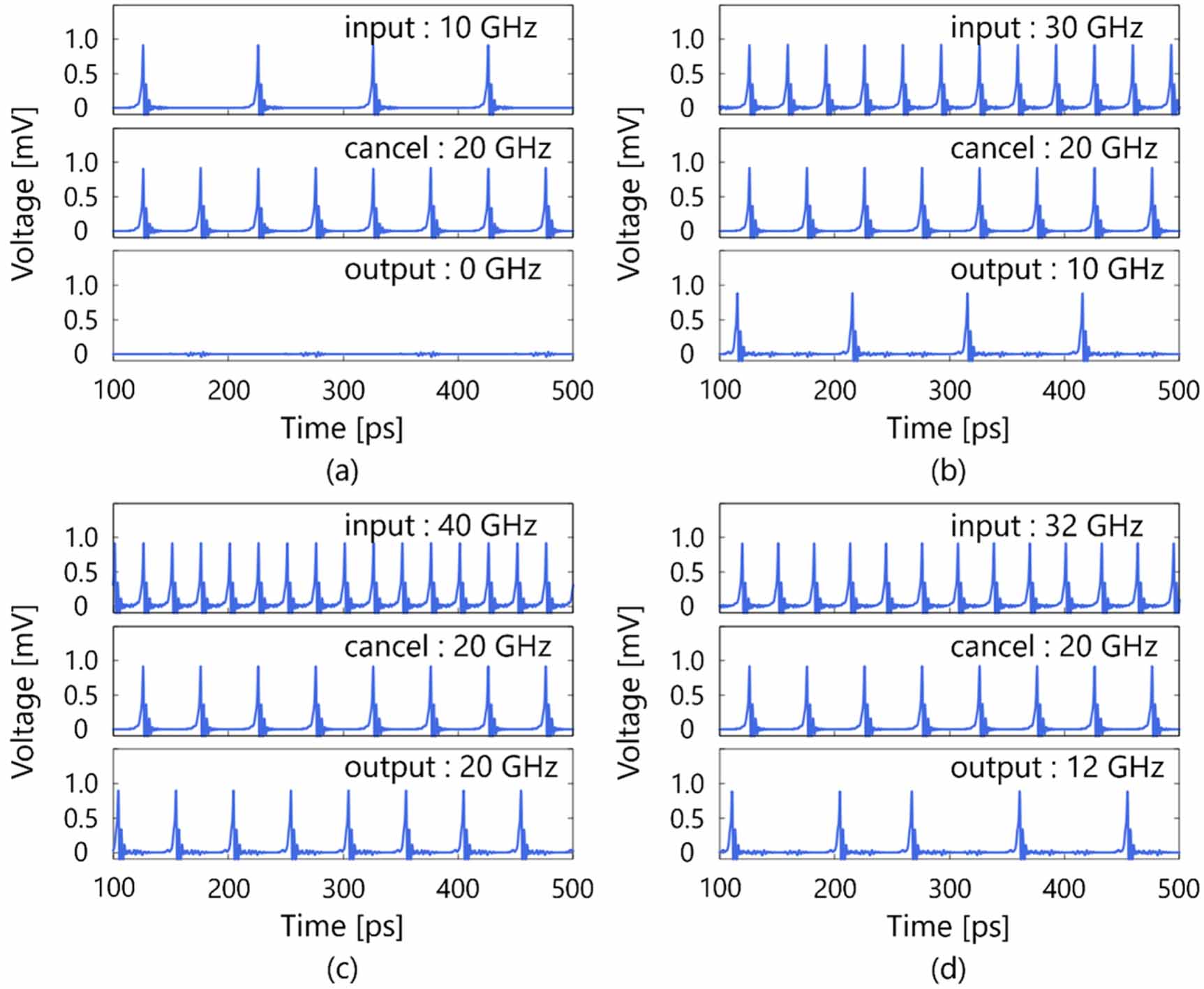
Figure 3 shows the transient analysis results of the designed neuron circuit when fcan is fixed to be 20 GHz. We used an analog circuit simulator JoSIM [33]. The use of the 10 kA cm−2 Nb superconductive integrated circuit fabrication process provided by National Institute of Advanced (AIST) is assumed in this simulation. It can be confirmed that the SFQ signal is output from the ‘output’ port at the average frequency according to equation (1).
Figure 3. The simulation results of the proposed neuron circuit when (a) fin = 10 GHz, (b) fin = 30 GHz, (c) fin = 40 GHz and (d) fin = 32 GHz. fcan is fixed to be 20 GHz. SFQ output frequency in the figures are average frequencies for each input frequency.
Download figure:
Standard image High-resolution image 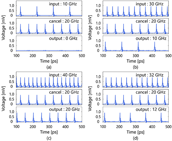
Figure 4 shows the simulated dependences of the average output frequency on the input frequency fin when fout = 10 GHz and 20 GHz. The solid lines are the ideal ReLU characteristic, and dots and triangles represent the simulated results. In our design the correct operation up to the input frequency of 47.6 GHz is obtained. In this design, the maximum operating frequency is limited by the reciprocal of the summation of latency of the RDFF output and delay time of the delay element. When the input frequency is above 47.6 GHz, the output SFQ signal has the same frequency as the input signal. When the clock frequency exceeds 47.6 GHz, the subsequent SFQ input is applied to the ‘din’ port of RDFF before the clock signal is input. Consequently, a ‘1’ is consistently output from the RDFF, synchronized with the clock input, resulting in identical output and input frequencies.
Figure 4. Simulated dependence of the output average frequency on the input frequency. Solid lines represent ideal ReLU characteristics.
Download figure:
Standard image High-resolution image 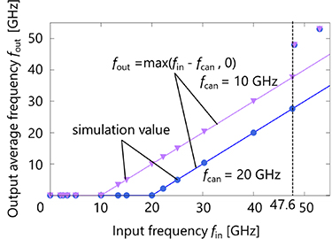
The proposed neuron circuit offers significant advantages in both high-speed operation and robustness to component parameter fluctuations. This exceptional robustness stems from the inherent optimization and design of general SFQ logic gates for parameter variation tolerance [34]. In our design, the Josephson junction in the RDFF has the minimum parameter margin of 24.9%. We confirmed through analog circuit simulations that the ideal ReLU input–output characteristic is maintained even when the 20% variation of the critical current of the Josephson junction in the RDFF is taken into account. This robustness stands in sharp contrast to conventional analog-based neuron devices, whose performance is highly susceptible to device non-uniformity. Furthermore, in superconducting circuits, the output voltage is precisely determined by the output SFQ signal frequency, offering accuracy sufficient for use as a voltage standard [35]. Consequently, the proposed circuit can achieve completely ideal ReLU characteristics even with minor circuit element variations. This characteristic is particularly advantageous for configuring large-scale neural networks comprising numerous neuron elements.
We designed a test circuit for the proposed neuron circuit utilizing the AIST 10 kA cm−2 Nb four-layer 1.0 μm high-speed standard fabrication process, we call the AIST-HSTP [36, 37]. We designed the circuit by the cell-based design methodology [38] using our cell library [34] modified for the AIST HSTP. The neuron circuit itself comprises 46 Josephson junctions. This number of connections is much smaller than that of large-scale SFQ circuits that have been demonstrated to date [39]. Therefore, there is no problem with the proposed neuron integration. The footprint of the neuron circuit is 160 μm × 160 μm, which corresponds to approximately 2% of our previous neuron circuit with sigmoid activation function [22].
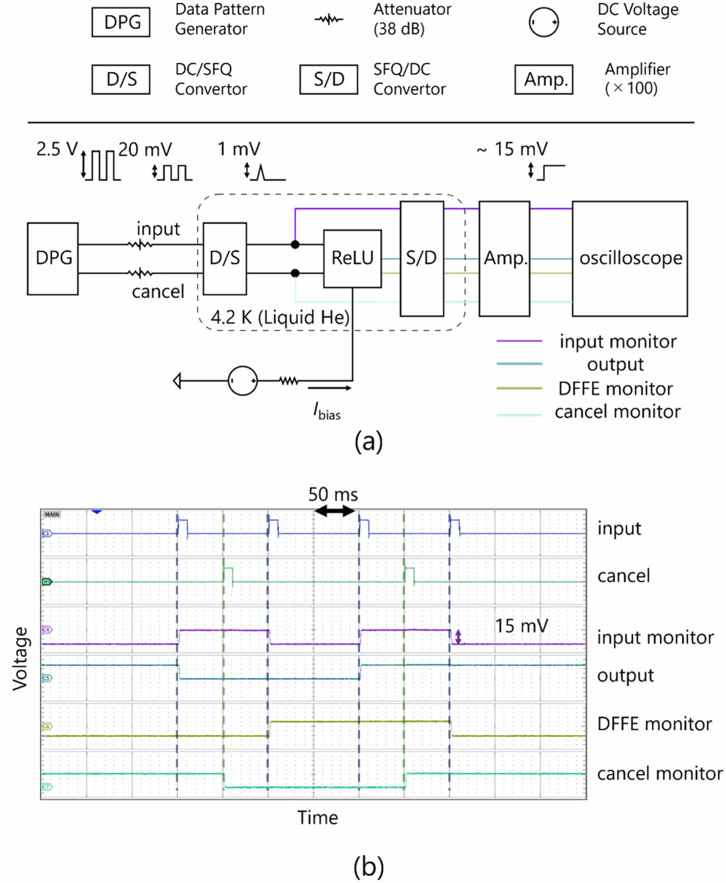
The test circuit was cooled and measured to 4.2 K by soaking the chip in liquid-helium. First, we performed the low-speed function test of the designed neuron circuit. Figure 5(a) shows the block diagram of the experimental setup for the low-speed test. All SFQ signals for low-speed test inputs were generated by a data pattern generator (Tektronix, DG2020A). Generated input voltages were input through attenuators (TAMAGAWA ELECTRONICS, UBA-641 C) to DC/SFQ converters [16], which convert the voltage inputs into SFQ signals. The output from the neuron circuit was measured via SFQ/DC converters [16], which convert SFQ input into voltage level transition. The output voltages were amplified 100-fold using differential amplifiers (Stanford Research Systems, SR560) and measured with an oscilloscope (IWATSU, DS-8018). The bias currents for the test circuit were supplied by the voltage source through room-temperature resistors. Figure 5(b) shows the example of the low-speed function test result. We confirmed the output based on the intended state transition. The measured dc bias margin, normalized bias voltage of our cell library, 2.5 mV [34], was −25.0%– + 24.4%.
Figure 5. (a) Block diagram of the setup for the low-speed function test. (b) The low-speed function test result of the neuron circuit. The output from the neuron circuit was measured via SFQ/DC converters [16], voltage level transition corresponds to SFQ signal outputs.
Download figure:
Standard image High-resolution image 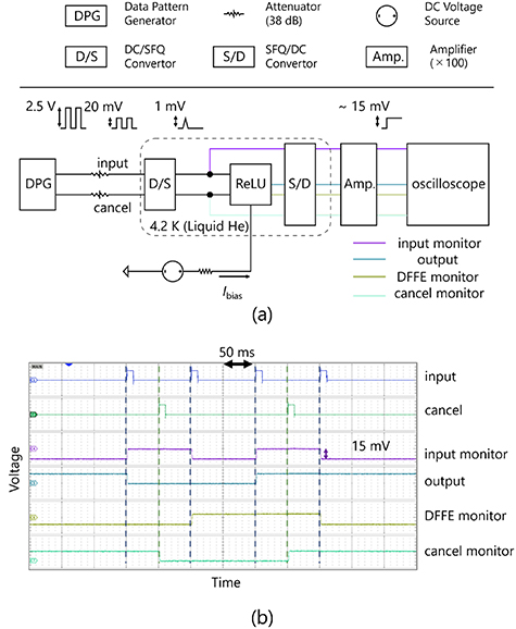
Figure 6(a) shows a block diagram of the high-speed test circuit, which comprises the neuron circuit (ReLU) and ring-oscillator-type clock generators (CGs) [16], and figure 6(b) displays a microphotograph of the fabricated test circuit. Continuous SFQ signals are produced by the CGs (CGin and CGcan) at frequencies ranging from approximately 10 GHz to 40 GHz. Each CG begins pulse generation upon receiving a trigger signal (CGin trig, CGcan trig) and stops operation when a corresponding stop signal (CG stop) is received. The test circuit, encompassing the CGs, signal wiring circuits, and signal interface circuit, integrates 462 Josephson junctions.
Figure 6. (a) Block diagram of the setup for the high-speed test. (b) Microphotograph of the implemented neuron circuit.
Download figure:
Standard image High-resolution image 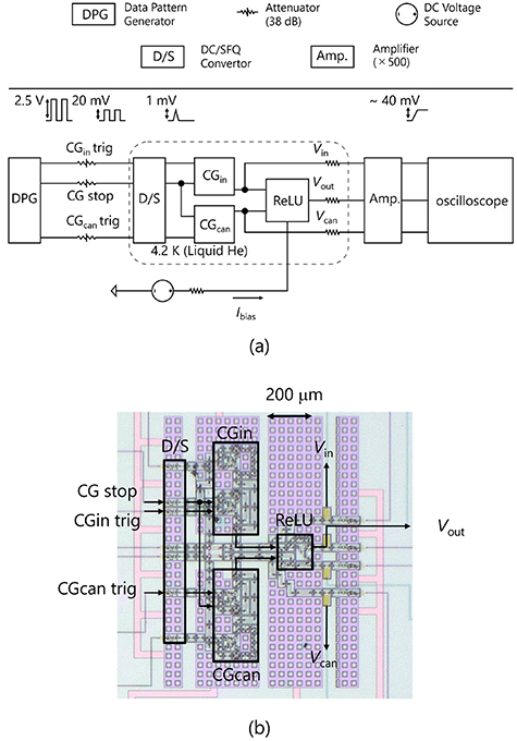
We measured the input–output frequency characteristics by assessing the average voltages of the CG outputs (Vin, Vcan) and neuron circuit (Vout) [40, 41]. The output voltages were amplified 500-fold using differential amplifiers and measured with an oscilloscope. Since the average output voltage, Vout, is represented by Faraday’s law:

We can determine the average output frequency from the average voltage outputs. We calculated the input and output average frequencies using equation (2), accounting for the 500-fold voltage amplification.
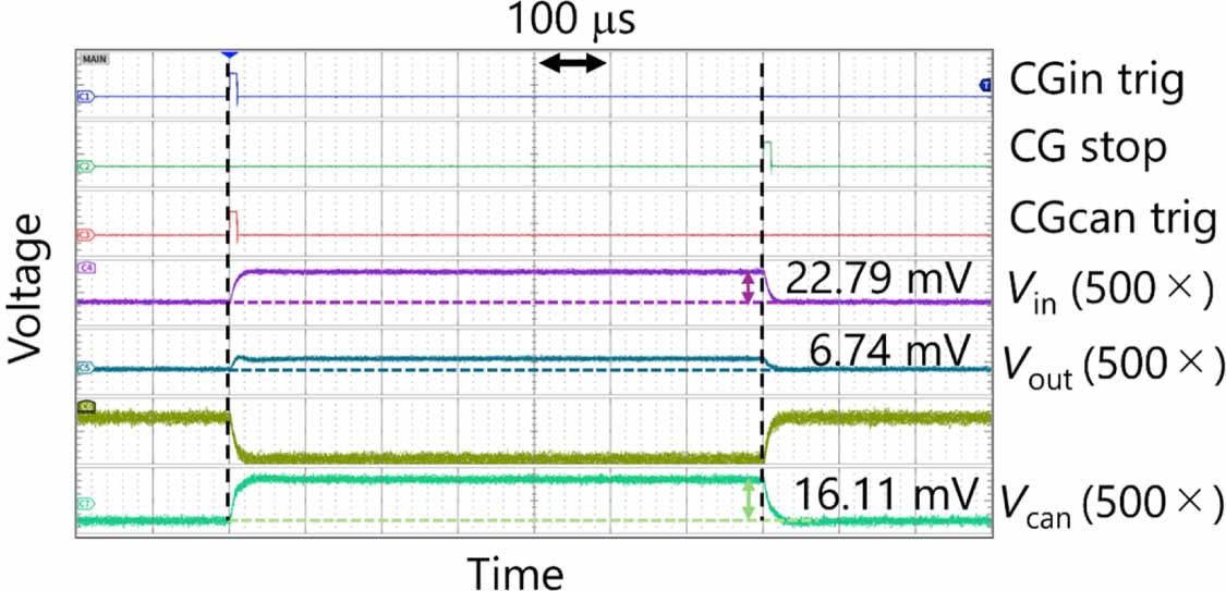
Figure 7 presents an example of the oscilloscope view obtained during high-speed measurement. Finite voltages (Vin, Vcan, and Vout) were observed only while the CG was operational. As the acquired voltage contained noise, the average voltage value during CG operation was utilized as the measurement. In this measurement, fin, fcan, and fout were 22.0 GHz, 16.1 GHz, and 6.5 GHz, respectively. The measured fout approximately agrees with the ideal output frequency (fin–fcan). We attribute the 0.1 mV error to measurement inaccuracies caused by noise and deviations from the nominal amplification rate of the operational amplifier because superconductive circuits can generate voltages with the same level of accuracy as voltage standards [35].
Figure 7. High-speed test result of the neuron circuit. When the CGs operate, the average voltages of input, cancel and output are 22.79 mV, 16.11 mV and 6.74 mV, were obtained, respectively. It corresponds to fin = 22.0 GHz, fcan = 15.6 GHz, and fout = 6.5 GHz.
Download figure:
Standard image High-resolution image 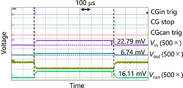
Figure 8 shows the measured output frequency dependence on the input frequency, derived from the high-speed test. We obtained these results from two different chips. In this test, the bias voltage supplied to CGcan was 2.5 mV, which is the standard bias voltage of our design. The measured oscillating frequencies of the CGcan (fcan) for chip1 and 2 were 15.6 GHz and 19.1 GHz for chip 1 and 2, respectively. According to the test element group measurement results, chip1 had manufacturing errors of approximately +13% in critical current of the Josephson junction and −17.0% in resistance value compared to the designed values. Chip2 had manufacturing errors of approximately +9.8% in critical current value and −18.0% in resistance value. The difference in the *f–*can between the two chips can be attributed to the difference in these parameters. However, both chips exhibit ideal input–output characteristics, which agree with the ReLU function. The experimentally obtained maximum operating frequencies for the two chips were 40.5 GHz and 41.2 GHz, respectively. This experimental maximum operating frequency is constrained by the upper limit of the CG oscillation frequency. The neuron circuit itself, however, can operate at higher frequencies, theoretically up to 47.6 GHz, as discussed in section 2.
Figure 8. The output frequency dependence on the input frequency from high-speed test.
Download figure:
Standard image High-resolution image 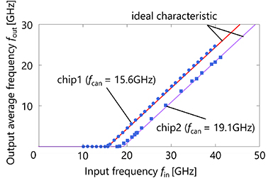
In this section, we compare our proposed device with those from other studies. The energy consumption per input, P, can be approximated using the following formula [42]:

where n is the number of Josephson junctions comprising the neuron circuit (46 in this design), f is the input frequency, and Ic is the average critical current of the Josephson junctions in the neuron circuit (150 μA in our design). We estimate the power consumption per neuron operation (NOp) as 100P, assuming 100 inputs at 40 GHz.
Table 1 provides a performance comparison of various neuron devices. Our proposed neuron circuit demonstrated the lowest energy consumption. Even when accounting for the cooling costs associated with achieving superconductivity, the overall power consumption remains at an extremely low level. Conversely, the physical area of our circuit is larger than other devices. This difference stems from the relatively early stage of integration in superconductive circuit fabrication processes; specifically, the minimum linewidth of the wire in our current design is only 1.0 μm [36, 37]. We anticipate that incorporating a more advanced circuit fabrication process, such as [43], will allow for a significant reduction in our neuron circuit’s footprint. Furthermore, as highlighted in section 3, our neuron circuit possesses inherent tolerance to device parameter variations, a distinguishing feature absent in many alternative components.
Table 1. Performance comparison of various neuron devices.
| | Activation | Energy (pJ/NOp) | Latency (ns) | Area ( ) | Tolerance to parameter variation |
| | ––––– | —————– | ––––––– | ———————————————————————————————————————– | –––––––––––––––– |
| This worka | ReLU | 0.0014 (0.56)b | 10 | 25 600 | Yes |
| Mott [6] | ReLU | 199.5 | 61.4 | 0.64 | No |
| Spintronic [11] | Sigmoid | 0.508 | 50 | N/A | No |
| SFQ [22] | Sigmoid | N/A | N/A | 1260 000 | No |
| CMOS [44] | ReLU | 316.7 | 17 | N/A | No |
| Photonic [45] | ReLU | 37.5 | 0.01 | N/A | No |
) | Tolerance to parameter variation |
| | ––––– | —————– | ––––––– | ———————————————————————————————————————– | –––––––––––––––– |
| This worka | ReLU | 0.0014 (0.56)b | 10 | 25 600 | Yes |
| Mott [6] | ReLU | 199.5 | 61.4 | 0.64 | No |
| Spintronic [11] | Sigmoid | 0.508 | 50 | N/A | No |
| SFQ [22] | Sigmoid | N/A | N/A | 1260 000 | No |
| CMOS [44] | ReLU | 316.7 | 17 | N/A | No |
| Photonic [45] | ReLU | 37.5 | 0.01 | N/A | No |
aThe latency and power consumption are estimated assuming 100 SFQ signal inputs and 40 GHz operation. bEnergy consumption is considered to be 400 times higher than the power consumption of the device [46].
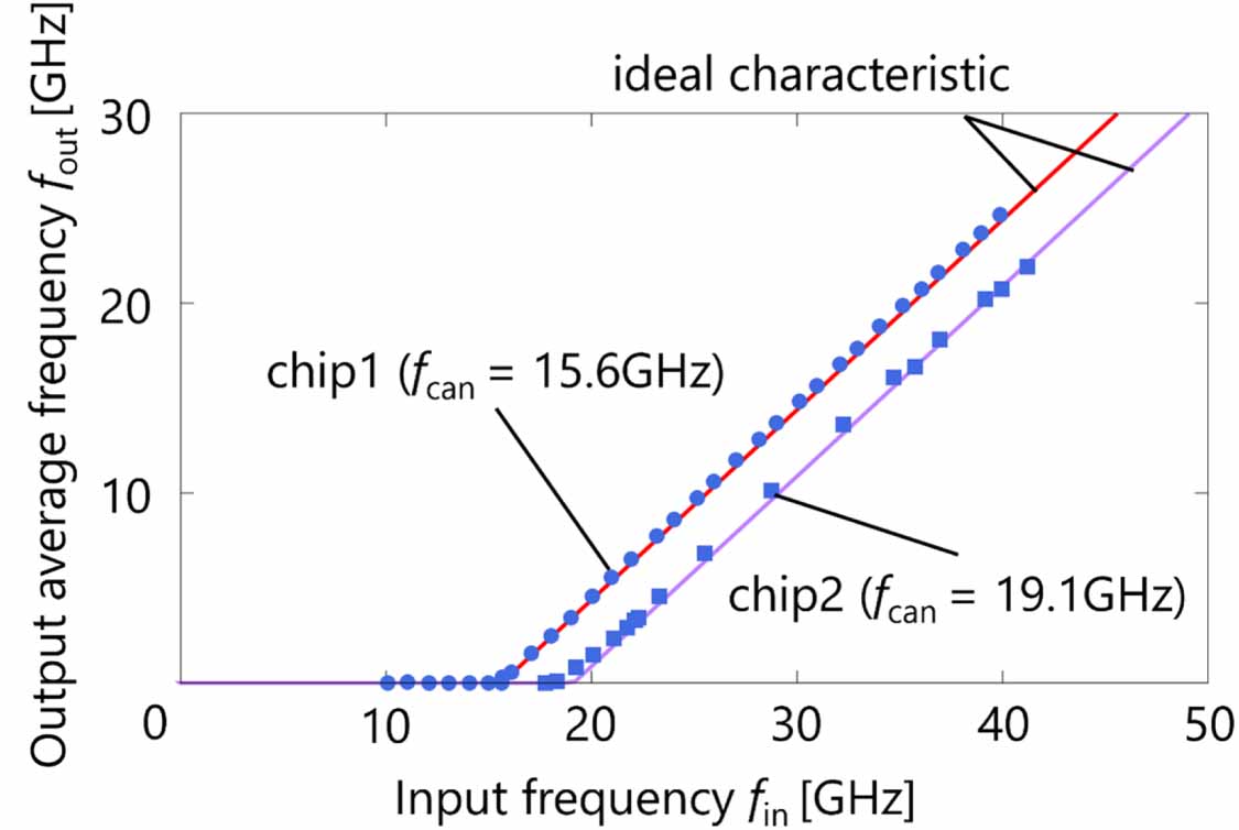
Figure 9 shows the proposed superconducting SFQ neural network, which integrates the circuit described herein. Synaptic weights in this network are realized using a Josephson current comparator, a fundamental building block of SFQ circuits. The ‘1’ output probability of this comparator can be continuously modulated from 0 to 1 by an external current, Iweight [20], thereby enabling its function as a weighting circuit within the neural network. As depicted in figure 9, the proposed neuron circuits can be directly interconnected using only SFQ circuits, eliminating the need for semiconductor circuit components. Given that the Josephson comparator can operate at input frequencies exceeding 40 GHz with a 10 kA cm2 Nb fabrication process [21], neither the weighting circuits nor the SFQ network circuit itself will impose limitations on the maximum operating frequency of the entire neural network system.
Figure 9. SFQ Neural Network employing the proposed circuit. The ‘W’ element represents Josephson current comparators, which function as weighting circuits within this network. The confluence buffer, which is represented by a circle before the ‘W’ element is the signal merging circuit in the SFQ circuit [16].
Download figure:
Standard image High-resolution image 
Furthermore, on-chip learning could be achieved by feeding the output back to the weight control input via SFQ digital-to-analog converters [47]. Implemented entirely with SFQ circuits, this approach offers high scalability and extensibility. The construction of the entire neural network exclusively from superconducting circuits enables extremely low power consumption for the whole system. Considering these unique attributes, we believe our devices hold significant promise for future large-scale, high-performance neural network circuits.
We proposed a neuron device that uses a superconductive SFQ circuit and features a ReLU activation function. This neuron device stands out because it operates at high speeds with ultra-low-power consumption and is tolerant to parameter fluctuations during circuit fabrication. We also anticipate its application in large-scale, high-speed superconductive neural network circuits, as it offers area savings compared to our previous designs. The proposed circuit is theoretically capable of operating correctly at input frequencies up to 47.6 GHz when manufactured using currently available superconductive integrated circuit fabrication processes. We experimentally verified its correct operation at input frequencies up to 41.2 GHz. Furthermore, measurements from two different chips have demonstrated its resistance to circuit parameter variation. We believe this circuit has the potential for significant contributions to high-performance neuromorphic computing with superconductive circuits.
This work was supported by JSPS KAKENHI under Grants 24H00311 and 25K01284. The circuits were fabricated in the Superconducting Quantum Circuit Fabrication Facility (Qufab) in National Institute of Advanced Industrial Science and Technology (AIST).
All data that support the findings of this study are included within the article (and any supplementary files).