AMD’s extant "X3D" processors include a feature called 3D V-Cache, which involves bonding a slab of SRAM cache to the logic die in such a way that it physically extends the L3 cache of the CPU to triple its original capacity. What if we could do the same thing for L2 cache? AMD may actually be investigating that, as one of its employees filed a patent back in 2024 about doing exactly that.
The patent, US20260003794A1, describes a method for "Balanced Latency Stacked Cache". You see, the idea of stacking on extra L2 cache is fairly straightforward; from simply saying it above, you probably intuitively understood what we’re talking about [if you understand 3D V-Cache](https://hothardware.com/reviews/3d-vcache-entry-gra…
AMD’s extant "X3D" processors include a feature called 3D V-Cache, which involves bonding a slab of SRAM cache to the logic die in such a way that it physically extends the L3 cache of the CPU to triple its original capacity. What if we could do the same thing for L2 cache? AMD may actually be investigating that, as one of its employees filed a patent back in 2024 about doing exactly that.
The patent, US20260003794A1, describes a method for "Balanced Latency Stacked Cache". You see, the idea of stacking on extra L2 cache is fairly straightforward; from simply saying it above, you probably intuitively understood what we’re talking about if you understand 3D V-Cache.
A key thing to understand about AMD’s 3D V-Cache is that it was a big deal specifically because of the 3D part. It’s not called that because it helps with 3D games. It’s called that because it literally involves stacking a second chip on top of (or underneath, as is the case now) the first. You see, microprocessors are made in 2D, on a plane, so physically stacking SRAM in 3D with logic is rather unusual. Not novel, not "never done before"—but certainly rare in consumer products.
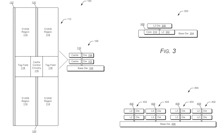 Three figures from the AMD patent, illustrating the structure of the idea.
The main reason 3D stacking hasn’t been applied to L2 already is because it wasn’t necessarily clear that you could deliver a meaningful performance improvement. L2 cache operates at such a rapid speed, with such short timelines, that the distance of the wires connecting the cache to the CPU logic becomes a major factor in performance, even at lengths measured in microns. When you’re stacking cache, it takes extremely careful design to make the cache usefully fast, even with L3. With L2, it’s an entire other level of challenge.
That’s why this AMD patent is so fascinating. In it, the author Carl Dietz describes the ability to stack L2 cache in such a way that it offers both reduced latency and power consumption versus a planar cache of the same size. It actually makes sense, if you think about it. The latency is largely the result of distance, and the shortest linear distance to an object remains the same regardless of what direction you’re going in. By putting 1MB of cache alongside a CPU core, and then 1MB of cache above it, you can achieve lower latency than putting 2MB alongside.
There’s more going on here than just that, though. The patent also describes the ability to stack on multiple cache dies, whether entirely for L2 cache, for L2 and L3 cache, or indeed multiple dies containing both. By routing the cache control circuitry through a central pillar, it becomes possible to do such multi-layered stacking. In fact, the illustrative figures in the patent go so far as to suggest that AMD could use as many as sixteen different stacked cache dies on a single processor.
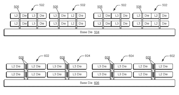 Figures from the AMD patent describing the use of many stacked cache dies.
Would AMD do such a thing? Certainly not on a Ryzen part; the manufacturing cost would blow up margins. It might make sense on ultra-expensive processor products intended for datacenter use, though, and we could certainly see a single layer of stacked L2+L3 on consumer products. The existing 3D V-Cache uses an SRAM die that does not cover the entirety of the Ryzen CCD (see the photo at the top), requiring the use of "dummies" to stabilize the processor. Expanding that die to include L2 for the CPU cores, which are situated on the outer edges of the CCD to begin with, makes a lot of sense.
So what would be the performance implications of such a thing? Potentially enormous, but also very workload-dependent. L2 cache sits right at the crossroads between raw execution speed and memory latency, and it’s often the first real bottleneck a hot core runs into once instruction-level parallelism is exhausted. Making L2 both larger and no slower—or even marginally faster, as the patent suggests—is one of those rare architectural tricks that doesn’t just help one narrow benchmark. It could improve instruction fetch, reduce pressure on L3, smooth out worst-case latency spikes, and generally let the CPU spend more time doing useful work instead of waiting on data that’s only a few millimeters too far away.
That said, this is still a patent, not a product roadmap, and patents are where engineers are allowed to dream out loud with math and diagrams. Whether AMD ever ships stacked L2 cache will come down to cost, yield, thermals, and whether the real-world gains justify the extra manufacturing pain. So, the important takeaway isn’t that "stacked L2 is coming," but rather that AMD is clearly thinking beyond simple cache enlargement and toward a future where how far electrons actually have to travel matters just as much as clocks and cores. The flat era of CPUs is finally ending, and the next big gains may come not from going faster or wider, but from going up.
Thanks to WCCFTech for the spot!

A 30-year PC building veteran, Zak is a modern-day Renaissance man who may not be an expert on anything, but knows just a little about nearly everything.